

How To Make A Register File That Holds 8 Words (Has 8 Registers) Of 4ã¢â‚¬âbit
The register is the main part of the microcontrollers and processors that provide a fast way to collect and store data. If we want to manipulate data with a controller or processor by performing add-on, subtraction, so on, nosotros cannot do that direct in the memory, but it needs registers to process and shop the data. Microcontrollers contain several types of registers that tin be classified according to their content or instructions that operate in them.
Different Types of Registers in the 8051 Microcontroller
Annals
A register is a minor place in a CPU that can store small amounts of the data used for performing diverse operations such as improver and multiplication and loads the resulting information on the principal retentivity. Registers comprise the accost of the memory location where the data is to be stored. The size of the annals is very important for modern controllers. For instance, for a 64-bit register, a CPU tries to add together two 32-bit numbers and gives a 64-flake result.
Types of Registers
The 8051 microcontroller contains mainly 2 types of registers:
- General-purpose registers (Byte addressable registers)
- Special office registers (Bit addressable registers)
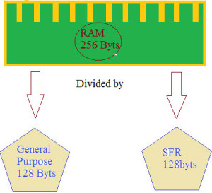
The 8051 microcontroller consists of 256 bytes of RAM, which is divided into 2 means, such every bit 128 bytes for general purpose and 128 bytes for special part registers (SFR) memory. The memory which is used for general purpose is chosen every bit RAM, and the memory used for SFR contains all the peripheral related registers similar Accumulator, 'B' register, Timers or Counters, and interrupt related registers.
General Purpose Registers
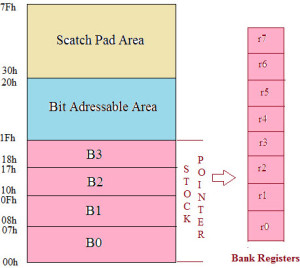
The general-purpose retention is called as the RAM of the 8051 microcontrollers, which is divided into 3 areas such as banks, bit-addressable area, and scratch-pad area. The banks incorporate unlike general-purpose registers such as R0-R7, and all such registers are byte-addressable registers that store or remove only ane-byte of data.
Banks and Registers
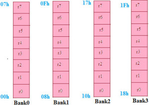
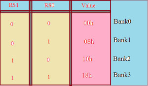
The B0, B1, B2, and B3 stand for banks, and each bank contains viii full general-purpose registers ranging from 'R0' to 'R7'. All these registers are byte-addressable. Information transfer betwixt general-purpose registers to general-purpose registers is not possible. These banks are selected by the Program Status Word (PSW) annals.
PSW (Program Status Word) Register
The PSW register is a chip and byte-addressable register. This register reflects the condition of the operation that is carried out in the controller. The PSW register determines bank pick by an RS1 and RS0, as shown below. The physical address of the PSW starts from D0h and the private bits are accessed with D0h to D7h.
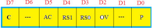
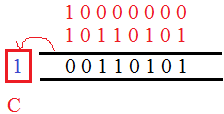
Behave Flag (C): The Accost of the Carry flag is D7. This acquit flag is affected when the fleck is generated from the 7th position.
When C=0 carry resets
C=1 behave sets
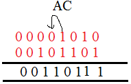
Auxillary Flag(Air-conditioning): The address of the auxiliary acquit is D5. This auxiliary carry is affected when a bit is generated from the 3rd position to the 4th position.
Air conditioning=0 auxiliary is reset
AC=1 auxiliary is set up
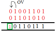
Overflow Flag (OV): The address of the overflow flag is D2. When a chip is generated from the 6th position to the 7th position, so the overflow flag is affected.
OV=0 overflow flag resets
OV=one overflow flag sets
Parity Flag (P): The address of the parity flag is D0. While performing arithmetic operations, if the result is 1, then the parity flag is set – otherwise, reset.
RS1 and RS0
The RS1 and RS0, the bits in the PSW annals, are used to select different memory locations (bank0 to bank4) in the RAM.
The following is an case of using this register.
The post-obit case demonstrates the addition of two numbers then the storage of concluding value in the Bank1 register using an associates level program.
Org 0000h
MOV PSW,#00h
MOV A, fifteen
Add A, 20
MOV 00h, A
END
Assembly program to move vi natural numbers in bank0 register R0-R5
Org 0000h (starting addresses announcement)
MOV PSW, #00h (open the bank0 memory)
MOV r0, #00h (starting address of bank0 retentiveness)
MOV r1, #01h
MOV r2, #02h
MOV r2, #03h
MOV r3, #04h
MOV r4, #05h
END
Assembly program to move 6 natural numbers in bank1 register R0-R7
Org 0000h (starting addresses annunciation)
MOV PSW, #08h (open the bank1 retentivity)
MOV r0, 00h (value send to the bank1 memory)
MOV r1, 02h
MOV r2, 02h
MOV r2, 03h
MOV r3, 04h
MOV r4, 05h
MOV r5, 06h
MOV r6, 07h
MOV r7, 08h
END
Special Function Registers (SFR)
Special part registers are upper RAM in the 8051 microcontrollers. These registers incorporate all peripherally related registers similar P0, P1, P2, P3, timers or counters, serial port, and interrupts-related registers. The SFR retentiveness accost starts from 80h to FFh. The SFR register is implemented by bit-address registers and byte-address registers.
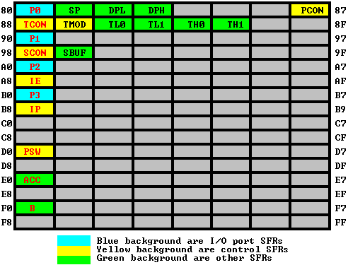
Special Function Registers (SFR)
The accumulator, B register, Po, P1, P2, P3, IE registers are bit-addressable register remaining all are byte-addressable registers.
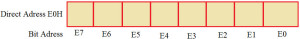
Accumulator
The accumulator which is too known equally ACC or A is a chip likewise as a byte-addressable register by an accost of the accumulator. If y'all want to utilise a chip-addressable annals, you tin utilize a single bit (E0) of the register and y'all tin can employ an 8-bit of the accumulator every bit a byte-addressable register. The accumulator holds the results of most Arithmetic and logical operations.
The Assembly programme for subtraction used with an Accumulator
Org 0000h
MOV R0, #09h
MOV A, #03h (1byte data)
SUBB A, 01h (1byte data)
END
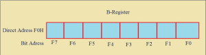
B-Annals
The B-register is a chip and byte-addressable register. You can access one-flake or all 8-bits past a physical address F0h. Suppose to access a bit 1, we accept to use f1. The B annals is only used for multiplication and division operations.
The Assembly programme for multiplication used with a B-Register
Org 0000h
MOV A, #09h
MOV B, #03h
MUL A, B (Final value stored in A)
Stop
The Assembly program for Sectionalization used with a B-Register
Org 0000h
MOV A, #09h
MOV B, #03h
DIC A, B (Final value stored in A)
Cease
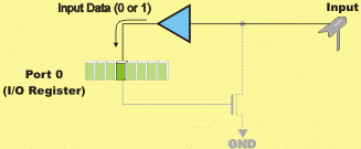
Port Registers
The 8051 microcontroller consists of 4-input and output ports (P0, P1, P2, and P3) or 32-I/O pins. Each pivot is designed with a transistor and P registers. The pin configuration is very important for a microcontroller that depends on the logic states of the registers. The pin configuration every bit the input given by 1 or output 0 depends on the logic states. If logic 1 is practical to the chip of the P annals, the output transistor switches off the appropriate pin that acts as an input pin.
Assembly program to toggle LEDs of Port0
ORG 0000h
RETURN: MOV P0, #00h
ACALL DEL1
MOV P0, #0FF
ACALL DEL1
SJMP RETURN
DEL1: MOV R2, #200
DEL: DJNZ R0, #230
DJNZ R2, DEL
RET
Cease
Counters and registers
Many microcontrollers consist of one or more than timers and counters. The timers are used to generate precious time filibuster and the source for the timers is a crystal oscillator. The counters are used to count the number of external events – for instance, the objective counter, and the source for counters are external pulses applied beyond the counter pivot.
The 8051 microcontroller consists of two 16-bit timers and counters such equally timer 0 and timer 1. Both the timers consist of a 16-scrap register in which the lower byte is stored in the TL and the higher byte is stored in the TH. The Timer can be used as a counter equally well as for timing operation that depends on the source of the clock pulses to the counters.
The Counters and Timers in 8051 microcontrollers contain ii special function registers: TMOD (Timer Mode Register) and TCON (Timer Control Register), which are used for activating and configuring timers and counters.
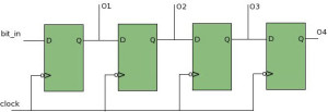
Types of Shift Register
Shift registers are a type of sequential logic circuits that are mainly used for the storage of digital data. The shift registers are scrap-addressable registers that store only one chip of data. The shift registers are constructed with flip-flops – a group of flip-flops connected as a chain then that the output from one flip-bomb becomes the input of the next flip-flop.
All the flip-flops are driven by the clock signals that are implemented past the D-flip-flap. The shift registers are mainly used for serial communication.
These are classified into 4- types:
- Serial in Serial out (SISO)
- Series in Parallel Out (SIPO)
- Parallel in Serial out (PISO)
- Parallel in Parallel Out (PIPO)
These are all unlike types of registers in an 8051 microcontroller. We hope that nosotros take successfully given you relevant content with the appropriate program for each annals. Furthermore, for whatsoever sort of help to know the coding of several other registers, you can contact u.s.a. by commenting below.
Photo Credits:
- Port Registers by mikroe
- D-Flip-flap Shift registers by electronicdesignworks

How To Make A Register File That Holds 8 Words (Has 8 Registers) Of 4ã¢â‚¬âbit,
Source: https://www.elprocus.com/know-about-types-of-registers-in-8051-microcontroller/
Posted by: overstreetquirld.blogspot.com
0 Response to "How To Make A Register File That Holds 8 Words (Has 8 Registers) Of 4ã¢â‚¬âbit"
Post a Comment